Olin Lathrop, Embed Inc.
Last modified 22 August 2008
Covered by US patent 7,411,378
Abstract
This paper discusses new approaches to controlling power factor correcting switching power supplies, made possible by the availability of low cost 16 bit microcontrollers with substantially more processing power than the previous generation. Replacing analog control electronics with digital processing power allows for wholly new control schemes not possible before.
The main focus of this paper is applying such techniques to power factor correction. It will be shown that feedback of the current is not required with the availability of divide and square root operations.
Examples will be shown using a Microchip dsPIC 30F2010 microcontroller. Details of this particular implementation will be presented.
This paper assumes you are familiar with electronics and have a basic understanding of switching power supplies, although a brief introduction to power factor correction is provided.
Introduction and Background
Traditional AC to DC power supplies, both switching and linear, usually start with a full wave bridge feeding a large energy storage capacitor as shown in figure 1.
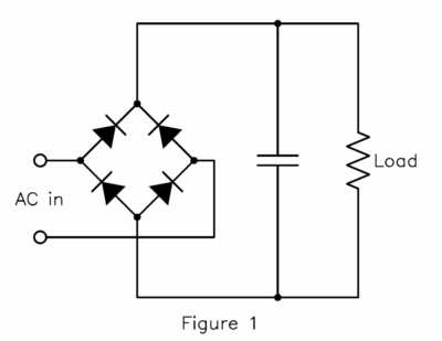
The capacitor is fully charged twice per power line cycle at the peak of the full wave rectified sine wave. A heavy pulse is drawn from the power line just before each peak, and no current at all at other times. The load is powered from the stored energy in the capacitor between the power line peaks. A sufficiently large capacitor maintains the load voltage constant to the level required by the load.
Figure 2 shows the various voltages and currents resulting from a simulation of the circuit in Figure 1. The power line voltage was 115V RMS at 60Hz, the capacitor was 500uF, and the load a 250 ohm resistor.
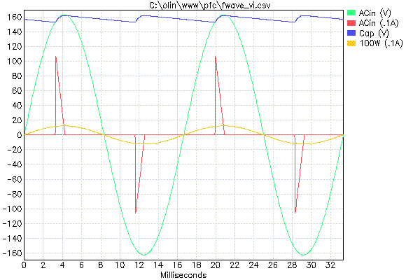
Figure 2
The green trace shows the AC power line input voltage. The red trace shows the current drawn by the full wave bridge circuit of Figure 1, with the blue trace showing the voltage on the storage capacitor. The power into the load in Figure 1 is about 100W in this example. The orange trace shows the current that would be drawn by a purely resistive 100W load connected directly to the power line.
Note that although the load being powered in Figure 1 is resistive, the load presented to the power line is far from resistive. A 100W resistive load would draw 870mA RMS with peak currents of only 1.23 amps. As can be seen from Figure 2, the full wave bridge draws peak currents exceeding 10 amps at the same power level.
- OK, that's a legitimate question. After all, full wave bridges and AC power lines have been around nearly since neolithic times and the world hasn't come to a stop. Just about all current televisions, VCRs, computers, and other electronic equipment contain a full wave bridge to make a DC voltage that is the input to one or more switching power supplies. The switching power supplies then provide the regulated DC voltages used by the rest of the system.
But, this is also the problem. Advances in power semiconductors and availability of cheap off the shelf control chips have made the popularity of switching power supplies explode in recent years. There are now many more of them than just a few years ago, and they now handle higher and higher power levels. The problems caused by these schemes have gone from a curiosity, to a minor annoyance, to a significant enough problem to get the attention of regulating agencies.
Regulations have already been enacted in the EU that constrict how far load current may deviate from a pure sine in phase with the voltage for some types of loads. These regulations will likely get tighter in the future, be applied to smaller loads, and spread to other regions.
Specifically, here are some problems:
- The generators at power plants inherently produce sine wave voltages. These generators function most efficiently when the load currents are also sine waves. Among other things, it allows for a constant torque on the generator shaft, minimizing mechanical stresses. If all the power was drawn as a short spike twice per line cycle, it would be like hitting the generator with a hammer twize per revolution. These generators are large machines capable of handling megawatts and powering whole cities, so that would be a large hammer indeed.
- Transformers and other power handling equipment can only handle currents up to some maximum peak level. A sine wave load current minimizes this peak current for a given power level. Conversely, more power can be delivered with the same equipment at the same peak currents when the load current is a sine wave. In the example of Figure 2, the peak current drawn by the full wave bridge was about 8.5 times higher than the peak current of a sine wave load at the same power level.
- Many of the losses in the power delivery and transmission system are proportional to the square of the current. A load that draws its power as large current spikes has a higher average squared current than a sinusoidal load. This causes wasted power in the transmission system.
- A non-sinusoidal load on the power line eventually causes the power line voltage to deviate from a pure sine because the power line does not have zero impedence. These non-sinusoidal voltages cause additional inefficiencies in transformers and other equipment.
- Any deviation from a pure sine wave means the signal contains harmonics, or other higher frequencies than the 60Hz power frequency. Large short spikes contain significant harmonic content at high frequencies. Some of these frequencies are in the radio range, causing power lines to act as radio transmitting antennas. This can interfere with radio communication and other nearby electronic equipment. If you think this is just a theoretical argument, try holding an AM radio near the power line coming into your house or near the fuse box.
- One approach is to insert a passive filter between the power line and the equipment drawing power in short spikes. The power line is then presented with a somewhat "smoothed out" load current. This kind of filter can be effective at reducing the radio frequency harmonics to acceptable levels, but would require prohibitively heavy, large, and expensive inductors to make the load appear anything near sinusoidal.
Current regulations specify the maximum level of radio emissions allowed from electronic equipment. Manufacturers generally install small passive filters at the power input. These reduce radio interference but do little to address the other problems mentioned above.
The same advances to power semiconductors that have lead to a proliferation of circuits that cause the problems mentioned above have also made a new solution feasible. This solution is generally called power factor correction, often abbreviated PFC.
- Power factor correction (PFC) is an active electronic technique to present a "nice" sinusoidal load to the power line regardless of the final load's characteristics.
There are a number of topologies for achieving this, with active research on many fronts. The examples in this paper focus on the boost-buck topology.
The PFC part is performed by a boost converter taking the raw rectified AC line as input. The boost converter switches at many times the power line frequency such that the power line voltage changes relatively little between each boost pulse. The boost converter produces a voltage somewhat higher than the highest peak of the AC input line. For each boost pulse, the average current drawn from the AC line for that pulse interval is proportional to the instantaneous AC line voltage. The current drawn from the AC line is therefore sinusoidal and in phase with the voltage. In other words, the load on the AC line appears resistive, which is the ideal case.
However, if the current drawn from the AC line is dictated by the AC line voltage, how is the boost switcher output voltage regulated or even controlled at all? The answer is that it is controlled, but much more slowly than at each switching pulse. In other words, the resistance of the resitive load presented to the AC line is slowly varied according to the demands of the final load. The line current is still mostly proportional to the line voltage, but this proportionality "constant" is slowly varied over a number of line cycles.
The output of the boost switcher is therefore a DC voltage a bit higher than the AC line peak voltage with significant ripple at twice the line frequency. This supply voltage is rarely useable directly. Most electronic circuits require a much lower and well regulated voltage. This is where the "buck" part of the boost-buck topology comes in. The boost output voltage becomes the input to a traditional buck regulator, which produces the regulated supply voltage used by the electronic circuit.
What's the big deal?
What's the solution?
The ABCs of PFC
The test platform circuit
The purpose of this paper is to discuss digital techniques of controlling a PFC circuit. A test platform was built to allow experimenting with different algorithms. This section describes the test platform, which will be used as the basis for subsequent discussion. The descriptions below refer to the schematic.- AC line power comes in at the top left to P1, P2, and P3. The circuit of R1, C1, D1, D2, C2, and D3 is a small charge pump to light LED D3 when input power is on. It is for safety and convenience and serves no other purpose.
The rest of the test board is isolated from the AC line by T1. This is for safety and convenience for experimenting and taking measurements. Real "production" PFC circuits are typcially connected directly to the AC line. Isolation, if necessary at all, is done at a later stage. For the rest of the circuit, the output of the T1 winding between pins 4 and 6 is considered the AC line.
The circuit immediately below and to the left of T1 only serves to light the LED D10 when the power is switched on. It is for safety and convenience and serves no other purpose.
R5 is a current sensing resistor, with P8, P9, and P11 test points for measuring the (isolated) AC line voltage and current.
C11, L1, and C12 are a filter to reduce the high frequency switching noise driven back onto the AC line.
D17, D18, D22, and D23 are the full wave bridge, producing the ACRECT line. This is the full wave rectified AC line that is the input to the PFC boost switcher.
The circuit in roughly the lower right quadrant produces several low voltage supplies derived from a 6.3V secondary of T1. These voltages are used to power the digital logic, the boost FET gate voltage, and the opamp used to drive the microcontroller A/D inputs. The terminal block connections "Aux +12V In", "Aux GND", and "Aux -12V In" allow the low voltage circuitry to be powered and tested with the AC line off. The diodes in series with these inputs allow the external +-12V supply to remain connected and on even when the AC line is switched on.
The small circuit in the top right corner provides the floating supply voltage for driving the buck gate FET. The "200V" line is the output of the PFC boost switcher, which is kept at a nominal 200V level. A P channel FET is used as the buck switching element, so the gate drive supply is about 16 volts negative with respect to the 200V line tied to the FET source pin.
- This is the boost converter that takes the full wave rectified AC line as input and produces a nominal 200V output. This is about as simple as it gets, even though this is the circuit that performs the actual power factor correction. The gate of the switching element Q1 is controlled by the BOOSTGATE signal entering at lower left. BOOSTGATE is driven directly by the microcontroller. Note the total lack of any kind of analog PFC control, including any current sense. All the control functions are implemented as firmware in the microcontroller, which will be discussed in a later section.
A fast recovery diode was chosen for D24 to allow for possible experimentation with continuous conduction mode. The algorithm discussed here uses discontinuous conduction at a fixed pulse frequency, and D24 has no need to be fast recovery in this case.
- This page shows the buck converter that starts with the weakly regulated nominal 200V output of the PFC boost switcher and produces a well regulated 12V out as an example.
This page looks a lot more complicated than it is, mostly because high side P channel FET drivers seem to be unavailable for some reason. An N channel FET driver could be used, except that such parts specifically drive the output low to ensure the N channel FET is off during power up. This would turn a P channel FET on during power up.
All the parts at the left and top of the page form a P channel FET driver. The details of this circuit aren't relevant to the overall discussion. The important part is that the FET gate is driven with high switching current from the 200V rail to about 10V less in response to the BUCKGATE signal going from 0 to 5V. The circuit also has the useful feature of no quiescient current when BUCKGATE is low and Q5 is off. The BUCKGATE signal is driven directly by the microcontroller.
R16, R17, and Q9 produce the BKPDONE signal into the microcontroller. This signal is driven low when diode D27 is reverse biased. This indicates that the flyback period of the previous buck pulse has ended. D27 is not a fast recovery diode, and a new pulse must not be started when it may still be conducting from the previous pulse.
- This page shows how the dsPIC 30F2010 microcontroller is connected.
At the left side, three analog voltages and a spare input are scaled to 0-5 volt range, then driven onto 4 separate A/D input pins. The three voltages (rectified AC line, 200V intermediate supply level, and final output voltage) along with the BKPDONE digital signal are the only inputs into the controller during normal operation.
The "motor control" PWM module of the dsPIC is used to produce the BOOSTGATE and BUCKGATE signals. These directly control the boost and buck FET gate drivers. These are the only outputs of the controller during normal operation.
The ICD-2 in-circuit debugger interface in the lower right corner, and the RX and TX serial lines are for debugging and to aid in experimentation. Neither is required for normal operation.
- This page shows the electrical details of how the 0-5V processor TX and RX signals are converted to the host serial RS-232 port. The host serial interface was provided on the test platform to allow for data collection and easy experimentation. A serial interface would certainly not be needed on a "production" PFC controller.
Page 1, Input power
Page 2, Boost converter
Page 3, Buck converter
Page 4, control processor
Page 5, Host interface
Power factor correction details
This section describes the details of the power factor correction algorithm. The job of this algorithm is to control the boost converter switching element such that the boost converter produces a nominal 200V internal supply while presenting a resitive load to the AC line.The use of digital computation instead of analog electronics to control a PFC switcher allows for different control schemes than are feasible in the analog domain. The algorithm presented here is an example of one such scheme.
The boost switcher is run in discontinuous mode at a fixed frequency of 25KHz. Discontinuous refers to the fact that the current thru L2 goes to zero for some time between each switching pulse. In other words, there is always some dead time between adjacent pulses.
The fixed frequency of 25KHz means that a new pulse is started every 40uS. The only variable that can be controlled per pulse is how long Q1 is left on for to charge up L2. This, together with the ACRECT voltage and the 200V line voltage define all the dynamic parameters of the pulse.
- The symbols used in subsequent discussions and equations are:
-
T1 = inductor charge time
T2 = inductor discharge time
Ti = total pulse duration (T1 + T2)
Tp = pulse period (40uS in example)
L = inductor inductance (2mH in example)
Vac = instantaneous rectified AC line voltage
Vo = output voltage (nominal 200V in example)
Imax = maximum inductor current during pulse
R = load resistance presented to the AC line
Figure 3 shows some of these symbols in a diagram of a pulse.
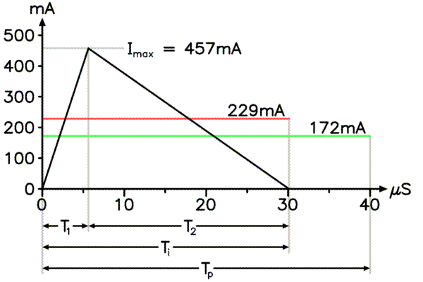
Figure 3
Click on figure to see animation over time.
Figure 3 diagrams an example boost pulse. The values are for the test platform circuit with 115V AC input at the peak of a power cycle with an average power draw of 14 watts. You can click on the figure to see an animation of the pulse parameters as they vary over time as a function of the rectified AC line input voltage.
During the T1 interval, the switching element Q1 is on and the inductor is being charged up from the AC line voltage. The slope of the current during T1 is therefore proportional to the line voltage. Q1 is switched off at the end of T1. The inductor current then has no place to go except thru D24 onto the 200V internal power rail. The slope during T2 is proportional to the difference between the 200V rail and the instantaneous AC line voltage.
The red line shows the average current during the pulse time Ti. The green line shows the same current averaged over the whole pulse interval Tp. This is the average current drawn from the AC line, and is the value that must be kept proportional to the AC line voltage by the PFC algorithm.
The problem therefore for each pulse is: Given the current values of Vac, Vo, and R, determine T1. The solution is:
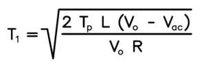
Note that 2, Tp, and L are constants, and that R is varied slowly by a seperate control algorithm. For the purpose of determining T1 each pulse, the equation can be re-written:
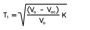
Where K is an arbitrary proportionality factor adjusted by another algorithm to control the 200V internal supply voltage. As long as K is changed slowly compared to the 120Hz full wave rectified power line, the current drawn from the line will be proportional to its voltage each Tp interval.
In fact, the values of L, Tp, and the resulting value of R are never computed nor known to the algorithm controlling the 200V internal supply. It simply adjusts K directly to achieve the desired result. If the 200V supply sags, K is adjusted upwards. If it is too high, K is adjusted downwards.
- This section discusses the details of the dsPIC implementation to solve for T1 every 40uS.
In this example, the dsPIC is run at 40MHz, which is 1/3 of its maximum speed. Even at this speed, there are 400 instruction cycles available per 40uS pulse period (25KHz pulse frequency). This is considerably more than adequate to perform the various computations for the PFC, control of the 200V internal supply, and the output buck switcher. Running the dsPIC at its full speed would therefore immediately allow for 75KHz switching frequency without any changes. It should be possible to achieve 100KHz switching speed (300 instructions) and still perform all computations each pulse interval.
The A/D sample time is ended and conversions begun at the start of each 40uS period. This also coincides with the start of the boost pulse, or time 0 in Figure 3.
An interrupt is generated when all A/D conversions are complete. The computation of T1 is performed during this interrupt. Channel 1 of the motor control PWM module is used to generate the boost FET gate signal, so the T1 result must be loaded into the PDC1 special function register before the start of the next pulse period.
This algorithm relies on the dsPIC's fast multiply capability. It can multiply two 16 bit values to produce a 32 bit result in a single instruction cycle. It also has hardware assist so that a 32 by 16 into 16 bit divide can be performed in 18 instruction cycles. The values Vo, Vac, K, and T1 are all 16 bit unsigned integers. The intermediate value of (Vo - Vac) * K is a 32 bits wide, which again becomes a 16 bit value after division by Vo.
Special care must be taken to ensure that the result of the division by Vo fits into a 16 bit number. This is done by scaling the denominator (Vo) up by factors of 4 until it exceeds the high 16 bits of the numerator. The number of times the denominator was multiplied by 4 is remembered, and the result of the square root is multiplied by 2 (shifted left one bit) the same number of times to compensate. Due to the dsPIC's barrel shifter, this last operation is performed in a single cycle.
The square root routine is the only part of the computation that had to be done "in software". Since the value to take a square root of is a 16 bit integer, the result is always an 8 bit integer. For now this routine is implemented by brute force, looping once for each of the 8 result bits. This could be optimized for a production implementation pushing the maximum possible pulse frequency.
The section of code that performs the T1 computation is shown below. The SQRT routine is not shown, but it computes the square root of the unsigned value in W0 and writes the result back to W0.
One additional detail is that Vo is computed as the measured 200V supply value plus the diode drop caused by D24. This is because the 200V line is measured, but Vo for the sake of the equation is the voltage on the other side of the diode. This is a minor tweak that is probably irrelevant compared to other system noise, but only costs two cycles.
         mov     ad_200v, w2 ;get 200V internal supply reading
        mov     #diodead, w1 ;get diode drop voltage
        add     w2, w1, w2  ;make effective boost switcher output voltage in W2
        mov     w2, vo      ;save it

        mov     ad_acrect, w1 ;get rectified AC voltage reading
        mov     #acrmul, w0 ;get mult factor to convert to 200V reading scale
        mul.uu  w0, w1, w0  ;make AC rectified voltage in 200V scale in W1
        sub     w2, w1, w0  ;make boost voltage difference in W0
        bra     nn, 1f      ;result is zero or positive ?
        clr     w0          ;negative, clip at 0
1:
;
;   The effective boost output voltage has been saved in VO, and the boost
;   difference voltage computed in W0.   W0 is guaranteed to be in the range
;   of 0 to AD_FSCALE, in the same units as the 200V supply A/D reading.
;
        sl      w0, #4, w0  ;scale for better range
        mov     k, w1       ;get current proportionality value
        mul.uu  w0, w1, w0  ;mult by proportionality value into W1,W0
        mov     vo, w2      ;get boost output voltage
        ;
        ;   W1:W0 contain the value to be divided by W2.   The square root of
        ;   the quotient will be the new value to write the PWM duty cycle
        ;   register.
        ;
        ;   However, the divide can only produce a 16 bit quotient.   To
        ;   guarantee the answer will fit into 16 bits, the denominator
        ;   in W2 is successively multiplied by 4 until it exceeds the
        ;   high word of the numerator in W1.   The square root of the
        ;   quotient is then shifted left 1 bit for each 2 the denominator
        ;   was shifted left.   This recovers the scale of the orignal
        ;   quotient.
        ;
        clr     w3          ;init number of times denominator shifted left by 2
1:                           ;back here to check if quotient fits in 16 bits
        cp      w1, w2      ;compare high word of numerator with the denominator
        bra     ltu, 2f     ;quotient will fit into 16 bits ?
        sl      w2, #2, w2  ;multiply denominator by 4
        inc     w3, w3      ;count one more time shifted
        bra     1b          ;back and check for 16 bit fit again
2:                           ;quotient will now fit into 16 bits

        repeat  #17
        div.ud  w0, w2      ;divide by output voltage into W0

        mcall   sqrt        ;take square root to make scaled pulse width in W0
        sl      w0, w3, w0  ;restore original scale

        mov     maxduty, w1 ;get max allowed duty cycle value
        cp      w0, w1      ;compare computed duty cycle to max
        bra     leu, 1f     ;computed duty cycle is within range ?
        mov     w1, w0      ;no, set to max allowed
1:                           ;clipped duty cycle value is in W0

        mov     w0, Pdc1    ;set boost switcher pulse width for next PWM period
;
;   The pulse width has been set for the next PWM period.
;
dsPIC details of T1 computation
200V internal supply regulation
The main focus of the test unit and the investigation was the PFC function. The other functions were implemented to serve as a testbed for the PFC function, and are not optimized nor claimed to be particularly clever. The regulation of the internal 200V supply is therefore only discussed briefly. It's implementation is merely intended to be "good enough".The important point of the 200V supply regulator is that it must not respond to individual 1/2 power line cycles. If it did, it would defeat the PFC function.
This also means that the energy storage capacitance on the 200V supply must be higher than if it were fed directly from the full wave rectified AC line. This would allow the capacitors to be recharged every 1/2 power line cycle. However, since the 200V supply controller must only respond to load changes over several power line cycles, the capacitors need to be considerably larger. This is one of the costs of a PFC implementation with unpredictable load. In this example, a total of 450uF was used (C15, C16, and C17).
To guarantee a sufficiently slow response, the measured level of the 200V line is low pass filtered before being presented to the controller. A three pole low pass filter is used. Each iteration, the value of each stage is moved 1/64 closer to its input value. The step response of the overall 3 pole filter is shown in Figure 4.
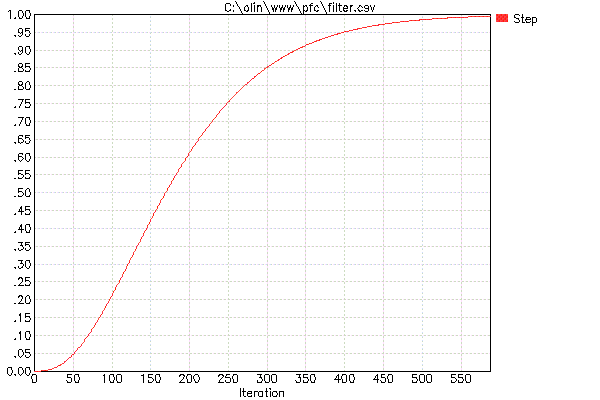
Figure 4
The filter constant (1/64) is deliberately the reciprocal of a power of 2 so that a multiply or divide can be accomplished by a bit shift, which the dsPIC can perform in a single cycle. A shift of 6 bits was chosen because this is the most a 10 bit A/D value can be shifted left and still fit in a 16 bit integer.
To not react much to individual power line cycles, the step response must be small after 1/2 power line cycle. At the 25KHz pulse rate, there are about 208 pulses in a 1/2 power line cycle. However as can be seen from Figure 4, the step response is over 60% after 208 iterations.
The solution used was to perform 50 filter iterations per 1/2 line cycle, which results in a step response of only 5% during that period. As a result, a filter operation is only performed every 4 or 5 pulses. The time since the last filter iteration is accumulated every pulse, and a new filter iteration performed when this time exceeds 1/50 of a 1/2 line cycle. This value in instruction cycles is precomputed by assembly time operations. When a new filter operation is performed, this value is subtracted from the accumulated time instead of resetting the accumulated time to zero. This guarantees the long term accuracy of the filter iteration frequency, although the period between iterations varies between either 4 or 5 pulses.
The result of the low pass filtered 200V supply voltage is compared to the desired value (200V) and K is adjusted accordingly. Again, K needs to be adjusted smoothly, so only small changes are made each filter iteration. The error (measured and filtered 200V supply value minus the desired value) is processed in two ways to produce incremental changes for K.
First, the direct error value times a fixed scale factor, GAINI, is subtracted from K. This means K is decreased if the 200V supply level is too high, and increased when it is too low.
Second, the derivative of the the error times a fixed scale factor, GAINP, is subtracted from K. This has the effect of dampening overshoots and undershoots. In other words, if the supply voltage is already heading in the right direction, don't change K as much as you would based on just the instantaneous value of the supply voltage alone.
The GAINI and GAINP values are assembly constants, and are adjusted up front. Their values select a tradeoff between the reaction time to transient load conditions, and the resulting size of the voltage excursions caused by those transients. In a nutshell, the GAINI and GAINP terms form a PI controller.
Since the incremental changes to K each filter iteration can be quite small, an additional 16 fraction bits are maintained for K. These fraction bits are only used by the K adjustment mechanism. The PFC algorithm uses only the upper 16 bits.
Results
Figure 5 shows the AC line voltage and current. For the purpose of the PFC circuit, the AC line voltage is actually the output of the transformer winding between pins 4 and 6.
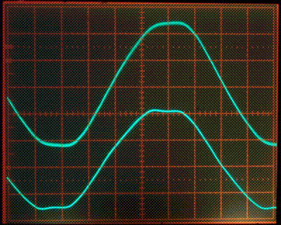
Figure 5
The top trace was measured from the "AC ref" to the "AC volt" test point, which is the AC line voltage from the point of view of the PFC circuit. Its scale is 50 volts/division.
The bottom trace is the voltage measured accross the current sensing resistor R5, filtered by a 2Kohm resistor and 100nF capacitor. This was done because the individual switching pulses are not fully attenuated by the C11, L1, and C12 filter. The remaining switching noise looked like a haze on the scope surrounding the current trace, making it difficult to see the real current waveform. The extra filter has a rolloff frequency of about 800Hz. This means it has little effect on the 60Hz signal up to the 10th harmonic, which is quite sufficient to see the general shape of the curve. The scale of the bottom trace is 200mA/division.
Clearly the current mostly follows the line voltage, meaning that PFC is being performed. There are also some noteable discrepancies:
- The voltage waveform itself is not a pure sine. The tops of the sine waves are visibly flattened. This is solely due to transformer T1. However, the PFC algorithm doesn't rely on a particular wave shape, and should make the input current follow the input voltage regardless.
- The current is leading the voltage a small amount. This is probably due to the filter capacitors C11 and C12, but has not been verified.
- The tip of the current waveform is even more flattened than the voltage waveform. The cause of this has not been determined yet and requires further investigation. The boost inductor L2 may be getting overloaded at the highest current levels.
Figure 6 shows the same signals with PFC disabled as a comparison. The boost switcher is never turned on, so the internal 200V supply line is just the full wave rectified AC line thru L2 and D24. The same load is connected to the 12V regulated output of the buck switcher.
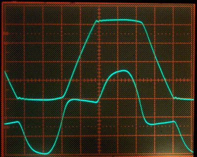
Figure 6
The relatively high impedence of transformer T1 and the high current draw at the tips of the waveform cause the voltage tips to be almost completely flattened. If the AC line voltage had a lower impedence, the current waveform would look more like the current in Figure 2. In any case, Figure 6 illustrates the highly non-sinusoidal current drawn by a traditional full wave bridge, and shows a clear contrast to Figure 5.
Conclusion
Direct digital control of switching power supplies and power factor correction circuits is here to stay, and will probably become the predominant method well within a decade. Control by a digital processor allows for new algorithms not workable with analog electronics.The PFC algorithm shown here is one such case. The PFC current feedback path is eliminated with the use of more computational power. While there are additional points to be investigated, the basic algorithm was demonstrated to work.
As processing power gets faster and cheaper relative to the power electronics it controls, more and more secondary effects can be modeled and corrected for. The algorithm presented here is only the beginning.
Không có nhận xét nào:
Đăng nhận xét